Numerical methods are essential for the accurate simulation and design of complex photonic components and lightwave circuits. Our group has a longstanding and extensive expertise in the development and application of advanced computational methods/techniques for simulating light propagation in photonic components and devices.
Developed methods include:
Developed methods include:
- Finite element method (FEM), 3D, time- and frequency-domain
- Finite difference time domain (FDTD) method
- Beam propagation method (BPM), FEM-based, full-vector
- Plane wave expansion (PWE)
- Eigenmode solvers, for waveguides and resonators
Areas of application span a broad range of guided-wave optical devices and free-space/thin-film devices. In the first class, we have a track record in integrated photonic and plasmonic waveguides, photonic crystals and photonic crystal fibers. Current research focuses on passive and tunable hybrid silicon-plasmonic components including both bulk and sheet (two-dimensional) materials like graphene. In the second class, our work has focused on liquid crystal displays, spatial light modulators and diffraction gratings.
References
- Chatzidimitriou D., Pitilakis A., Kriezis Em. E., "Rigorous calculation of nonlinear parameters in graphene-comprising waveguides," Journal of Applied Physics, 118, 023105, (2015). [pdf]
- O. Tsilipakos, Em. E. Kriezis, and T. V. Yioultsis, "Boundary condition for the efficient excitation and absorption of hybrid waveguide modes in finite element formulations," Microwave and Optical Technology Letters, 53 (11), pp. 2626-2631, (2011).
- O. Tsilipakos, A. Pitilakis, A. C. Tasolamprou, T. V. Yioultsis and Em. E. Kriezis, "Computational techniques for the analysis and design of dielectric-loaded plasmonic circuitry," Optical and Quantum Electronics, 42 (8), pp. 541-555, (2011).
- T. V. Yioultsis, G. D. Ziogos and Em. E. Kriezis, "Explicit finite-difference vector beam propagation method based on the iterated Crank-Nicolson scheme," Journal of the Optical Society of America A, 26, pp. 2183-2191, (2009).
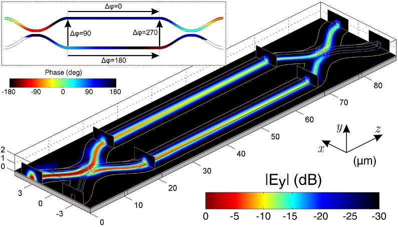
Fig. 1: Electric field distribution and phase-map along a DLSPP-based 2x2 MZI switch in the "bar" state, simulated with the FEM-based BPM.
(Click on image to enlarge)
Fig. 2: Finite element meshing of a waveguide cross-section. The graphene monolayer, depicted in red, can be modeled as (a) sheet/2D material or as (b) bulk/3D material.
(Click on image to enlarge)


